MIT Fired X-Rays Through a Chip to Watch Heat Move. A Single Micron-Wide Wrinkle Cut Heat Flow Fourfold
Existing methods can only read the top layer. Real devices have five or more. The new technique heats a sample with laser pulses and reads the buried layers with ultrafast X-rays.
Heat is the ceiling on modern chip design. Every increase in power density runs into the same wall: the device produces more heat than it can move out of itself, and performance is throttled to keep it from cooking. Designing around that requires knowing where inside a chip the heat actually gets stuck — and until now, the standard measurement tools could not see into the layers where it happens.
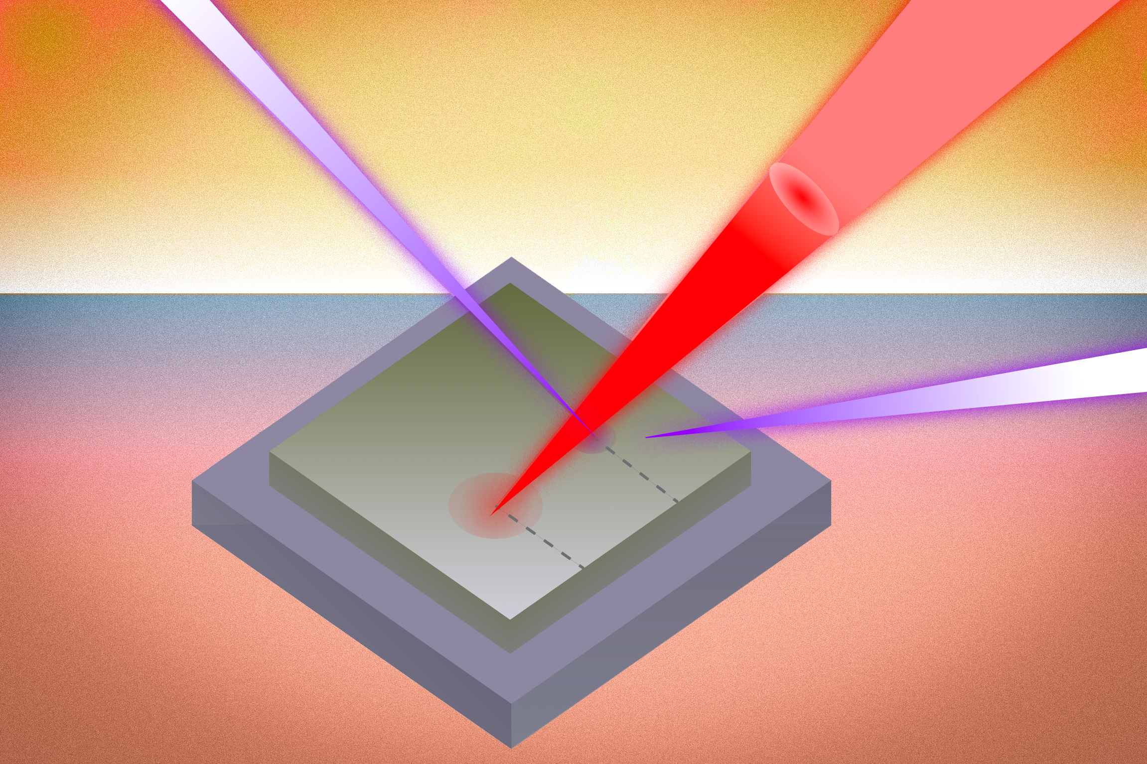
MIT researchers have published a technique in Nature Communications that reads thermal transport through a stack of buried layers rather than off the surface. The method pairs two things: laser pulses that deposit heat into the sample, and ultrafast X-rays that penetrate the layers and register how the material responds as that heat dissipates. Because X-rays go through the stack instead of bouncing off the top of it, the measurement resolves heat flow across interfaces that optical methods cannot reach.
The limitation being addressed is specific. Time-domain thermoreflectance, the workhorse optical technique, measures how a surface's reflectivity changes as it cools, which works well on a single film and poorly on anything else. Real devices have five or more layers, and the returning optical signal blends contributions in a way that makes buried interfaces effectively invisible. Interfaces are precisely where thermal resistance concentrates.
Applied to a gallium nitride layer grown over silicon — a combination of interest for both power transistors and flexible electronics — the technique produced a result that would have been hard to get any other way. The team measured the effect of a single micron-scale wrinkle in the material and found it reduced the ability to transfer heat at that spot by a factor of four, while also spreading heat unevenly around it. One defect, invisible at the device level, degrading local thermal performance by 300 percent.
"Chip developers need devices that can handle heat," said Mingda Li, the MIT associate professor who led the work with Jeehwan Kim. The team included postdoc Chuliang Fu and PhD candidate Mouyang Cheng among others. A leading semiconductor industry consortium has already approached the group about applying the method to other classes of chips.
The practical stakes sit in the same place as most current semiconductor bottlenecks: AI accelerators, which are power-dense by design and thermally limited in practice, along with wearables and power electronics for clean energy systems. A measurement that can attribute a fourfold local heat-transfer penalty to one micron-scale manufacturing defect gives process engineers something they can act on — a specific flaw with a quantified thermal cost, rather than a chip that simply runs hotter than the simulation said it would.