Air Holes Etched in Silicon Make Flat Ultraviolet Mirrors That Focus Light to a Micron
Stuttgart physicists turned silicon's strong UV absorption into an advantage, building half-millimeter mirrors from tiny elliptical cavities in a single etching step.

Lenses and mirrors have focused light with curved surfaces for centuries. Metasurfaces do the same job with a flat layer of nanoscale structures that locally control the phase of light. Extending that idea into the ultraviolet could support compact systems for high-resolution imaging, spectroscopy and sensing, but it runs into a basic materials problem: many of the materials used to make metasurfaces strongly absorb UV light. Researchers at the University of Stuttgart now report a way around it.
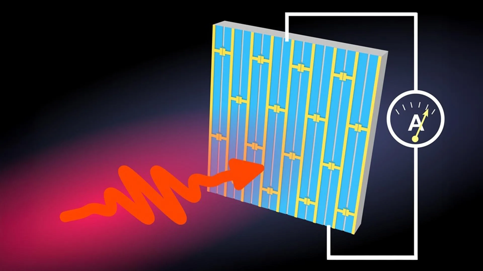
Instead of fighting absorption, they use it. Their device confines much of the light inside tiny air-filled cavities etched directly into silicon, so the light spends most of its time in air, where absorption is negligible, and little of it in the silicon that would swallow it. The team describes the structures, called Mie voids, in a paper in Advanced Photonics (DOI: 10.1117/1.ap.9.1.016002), and the first author is Julian Schwab.
Conventional dielectric metasurfaces rely on tiny pillars of a high-refractive-index material. Light gathers inside the pillars, and changes in their geometry steer the outgoing wavefront. Silicon works well for this at visible and longer wavelengths but turns strongly absorbing in the ultraviolet, so light trapped in a silicon pillar would simply be lost. Mie voids invert the design: rather than solid pillars surrounded by air, the researchers etch small air cavities into bulk silicon. Light entering a void reflects from the surrounding silicon boundaries and forms a resonant mode concentrated mostly in the air, which reduces the overlap between the optical field and the absorbing material.
Counterintuitively, silicon's strong UV absorption helps. The complex optical properties that come with absorption raise the reflectivity of the air-silicon interface, which keeps light confined in the void. The strategy does not eliminate absorption. It makes use of the optical properties of the absorbing material while keeping most of the resonant field away from it.
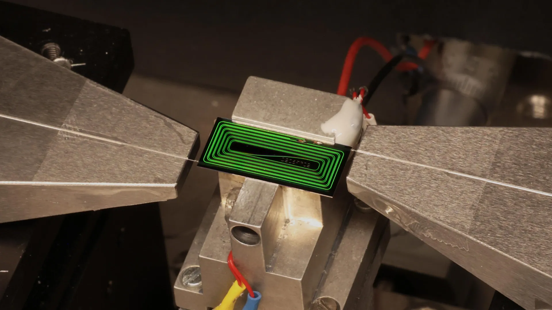
To turn the voids into a focusing mirror, the team shaped them as ellipses roughly 470 nanometers long and 100 nanometers deep. When circularly polarized light strikes an elliptical void, the reflected light picks up a geometric phase equal to twice the void's rotation angle. Varying that rotation across the half-millimeter-sized surface encodes a focusing profile directly into the silicon. Under an ordinary optical microscope, the arrangement shows up as colored ring patterns, so the encoded lens design is visible by eye.
The metasurfaces were tested at 325 nanometers, illuminated at a 45-degree angle, where they behave as flat equivalents of off-axis parabolic mirrors that redirect the beam by 90 degrees while focusing it. Devices with focal lengths from 5 millimeters down to 1.25 millimeters produced circular focal spots as small as about 1 micrometer. Up to a numerical aperture of 0.15, the spots approached the diffraction limit, the fundamental resolution bound set by the wave nature of light. By adding a spiral phase to the layout, the team also generated orbital angular momentum beams, in which light twists its phase around its axis and forms a doughnut-shaped intensity pattern.
The core advantage is simplicity. The metasurfaces are made in a single lithography and etching step on standard silicon substrates, compatible with established semiconductor processing, and the bulk substrate stays mechanically robust and sheds heat well. Because the mechanism tolerates and even benefits from material absorption, the authors say it can be extended into the deep and vacuum ultraviolet and applied to other material platforms. Since many biomolecules have characteristic UV absorption signatures, compact UV metasurfaces like these could eventually find use in integrated sensing.