Berlin Team Grows Lead-Free Polar Vortices on Silicon for the First Time
Alternating layers of barium and strontium titanate form regular stripes of electric-dipole whirlpools, a step toward putting exotic ferroelectric states on chip-industry silicon.

A team at the Helmholtz-Zentrum Berlin has, for the first time, reported polar vortices in superlattices of barium titanate and strontium titanate grown directly on silicon. The result, published in Nature Communications, widens the range of materials and substrates on which these swirling electrical patterns can form, and it points toward building complex ferroelectric states into silicon-based technology.
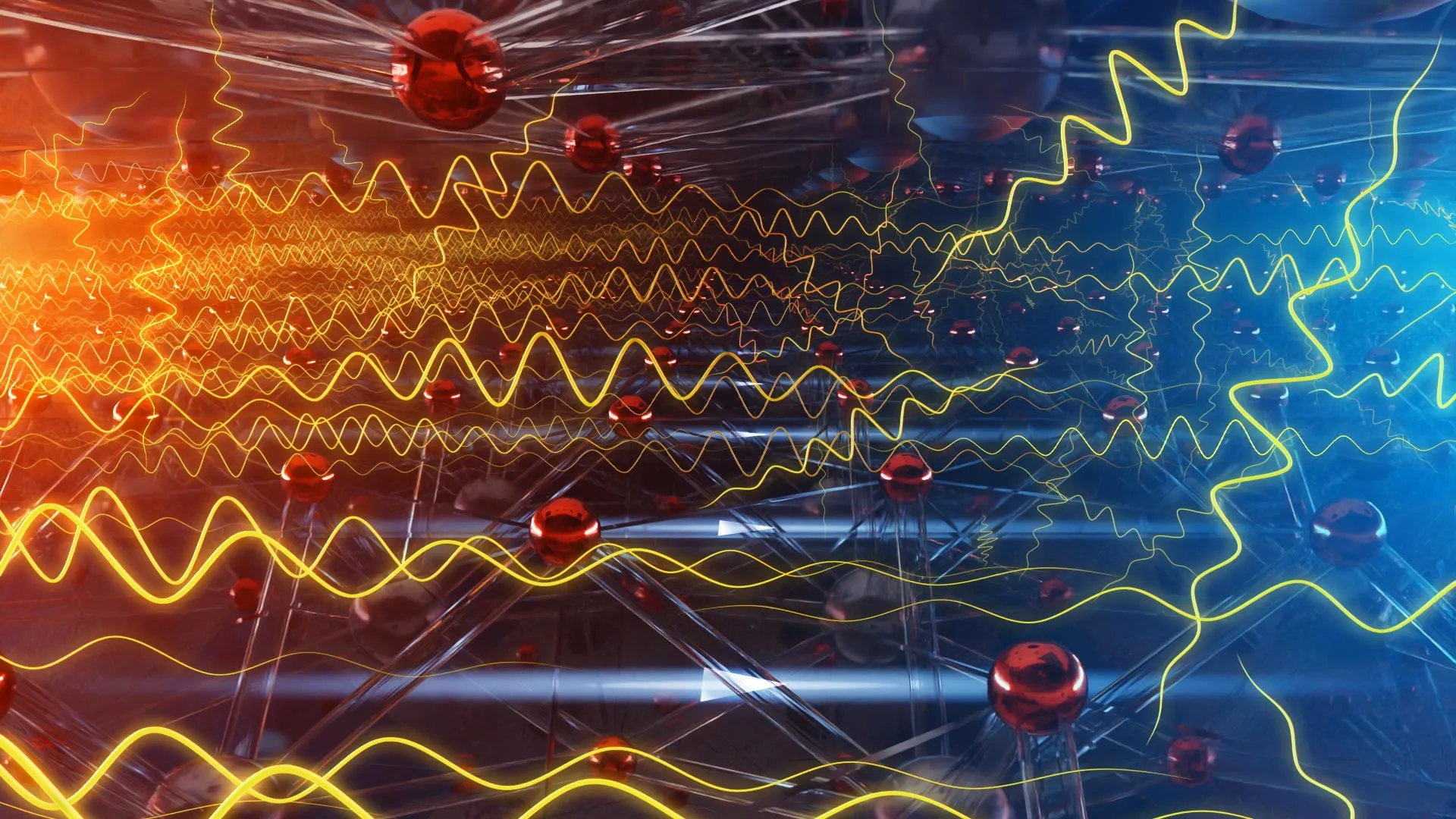
Polar vortices are textures in which the tiny electric dipoles inside a ferroelectric material curl around in loops, much as magnetic moments can in a magnet. Until now they had been seen almost exclusively in superlattices, stacks of ultrathin alternating layers, that contain lead, using titanate layers on oxide substrates. The textures arise from a delicate balance between electrical forces, the mechanical stress imposed by the substrate, and the energy needed to change the direction of polarization.
In principle, structures with such complex polar states could become components with specific functions. They are small, stable and can be influenced by external electric fields. But two obstacles stand in the way. The lead is toxic, and the layers need to sit on silicon, the ubiquitous platform of the semiconductor industry, rather than on specialty oxide crystals.
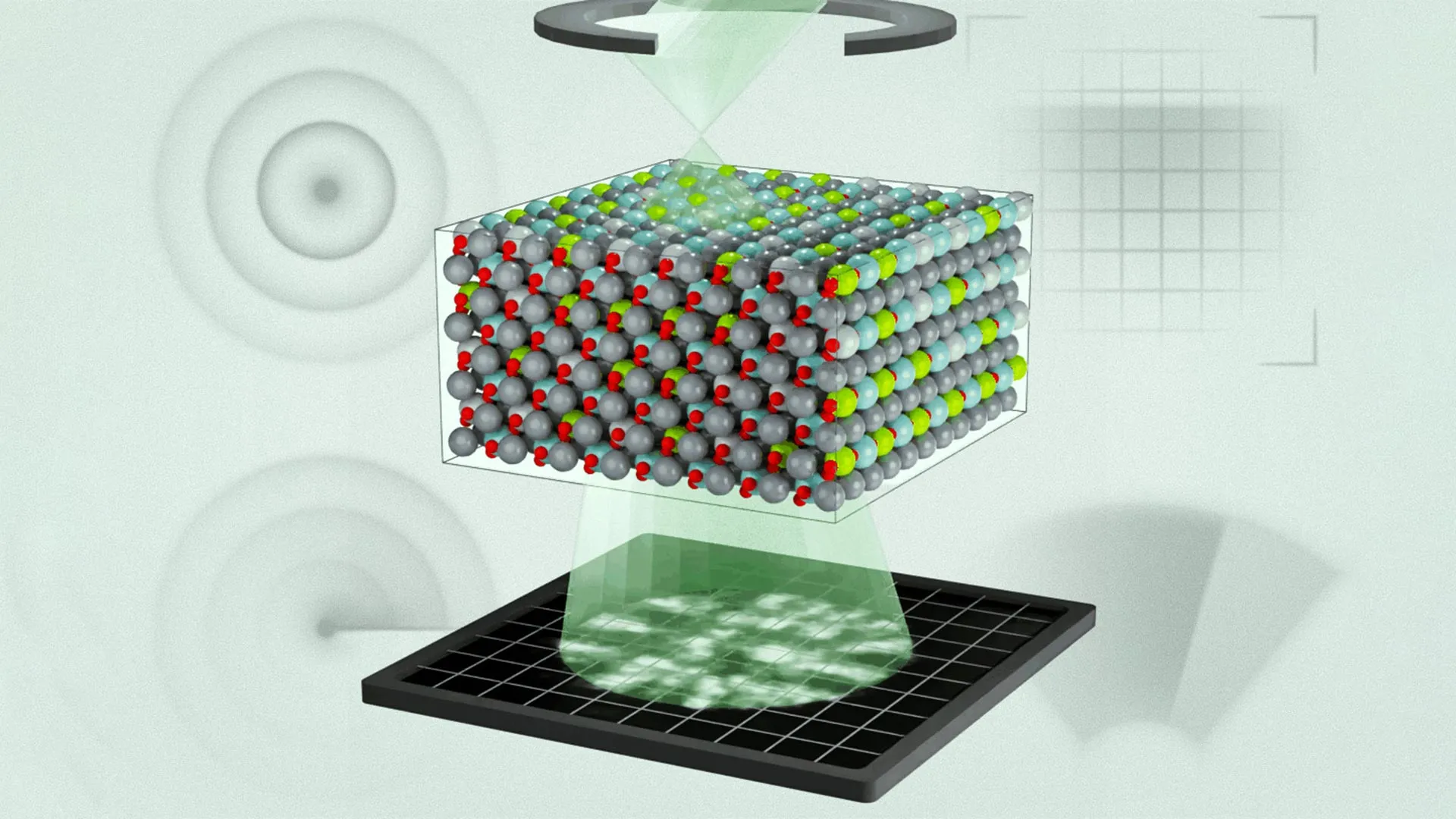
A team led by HZB physicist Catherine Dubourdieu has now cleared both. Her group grew epitaxial alternating layers of barium titanate and strontium titanate on silicon using molecular beam epitaxy in the HZB Quantum Materials lab. The superlattice has ten repeats and shows regular stripes of polar vortices. To prove the structure, the researchers used a scanning transmission electron microscope in the group of Christoph Koch at Humboldt University, and further analysis at the PETRA III X-ray source in Hamburg, which together revealed a superstructure of regular ferroelectric vortex tubes.
The vortices in each barium titanate layer line up along a particular crystal direction and form a robust striped pattern. Silicon turns out to be central to the effect. It supplies the mechanical strain that lets the vortices form. "This is the first realization of periodically ordered vortices in BaTiO3 superlattices on silicon," said Valentin Hevelke, a doctoral student and first author of the study. "Actually, silicon is the key, as it provides the necessary strain to induce this vortex pattern."
The pattern is also reversible. When the samples are heated, a structural phase transition occurs and the polar texture disappears. When they cool back to room temperature, the texture forms again. Phase-field modeling by the group of Long-Qing Chen at Pennsylvania State University reproduced how the barium titanate and strontium titanate layers couple through electrostatic forces and mechanical strain, and explained how the vortex tubes align as a function of strain.
"Our results expand the range of materials and substrates on which polar topological textures can occur and open up new options for incorporating complex ferroelectric states into silicon-based technologies," Dubourdieu said. The work is a materials demonstration, not a device, and the researchers do not claim a working component yet. But it shows that the vortex states need neither lead nor exotic substrates, which removes two of the biggest practical objections to using them.