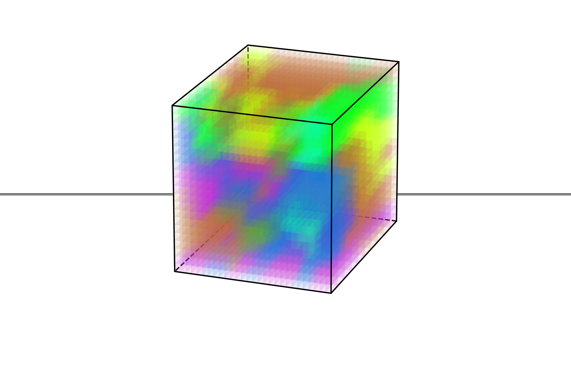
MIT Scientists Map Hidden Atomic Structure of High-Tech Electronic Material
Breakthrough imaging reveals three-dimensional structure of relaxor ferroelectrics, materials that power ultrasound machines and sonar systems worldwide.
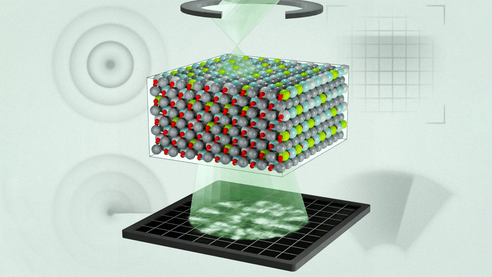
Researchers at MIT have achieved a historic breakthrough by mapping the three-dimensional atomic structure of relaxor ferroelectrics for the first time, solving a decades-old mystery about materials that are essential to modern medical and defense technologies. These materials have powered everything from medical ultrasounds to sonar systems for generations, yet their internal atomic arrangement remained largely invisible to scientists until now. The achievement, published in Science, provides the foundation for dramatically improving how these materials are designed and engineered for future applications.
Relaxor ferroelectrics derive their exceptional performance from complex atomic arrangements that have been extremely difficult to measure directly. Using an advanced technique called multi-slice electron ptychography (MEP), the MIT team examined a lead magnesium niobate-lead titanate alloy widely used in sensors, actuators, and defense systems. The method involves scanning a nanoscale beam of high-energy electrons across the material and recording diffraction patterns, creating detailed three-dimensional images of atomic-scale structures that were previously inaccessible.
The research revealed unexpected patterns in how electric charges are distributed throughout the material, challenging long-standing assumptions about these systems. "We realized the chemical disorder we observed in our experiments was not fully considered previously," explained co-first authors Michael Xu and Menglin Zhu, both MIT postdocs. Working with collaborators across multiple institutions, the team merged experimental observations with computer simulations to refine theoretical models and better predict material behavior under real-world conditions.
Corresponding author James LeBeau, MIT's Kyocera Professor of Materials Science and Engineering, emphasized the practical significance of understanding these atomic arrangements. "Now that we have a better understanding of exactly what's going on, we can better predict and engineer the properties we want materials to achieve," LeBeau noted. The improved models will enable researchers to design next-generation computing systems, energy devices, and advanced sensors with enhanced performance characteristics.
The breakthrough has immediate implications for multiple technology sectors that depend on relaxor ferroelectrics. Medical imaging systems could become more sensitive and accurate, while defense applications including submarine sonar could benefit from improved detection capabilities. The research also opens new possibilities for energy storage devices and precision sensors used in everything from smartphone cameras to industrial automation. As the research community continues developing methods to engineer these materials, the fundamental understanding provided by this atomic-scale mapping will serve as a crucial foundation for innovations that could transform how electronic devices interact with the physical world.