A Sub-Atom-Thick Layer of Iridium Manganese Boosts Spin Signals in Ultralow-Power Devices
Kyushu University researchers found that a 0.3-nanometer film, thinner than one continuous atomic layer, gave the strongest response. The finding could help devices that turn waste heat into electricity.

Researchers at Kyushu University in Japan have found that an ultrathin layer of iridium manganese, or IrMn, can improve two spin-related signals in a stack made of a magnetic insulator and a platinum film. By measuring how spin currents are generated and absorbed, the team gained insight into how such a layer helps spin cross a boundary, a result that could inform ultralow-power computing and energy harvesting devices.
Spintronics is a more complex approach to electronics that uses the spin of the electron, as well as its charge, to process and carry information. Researchers have spent decades looking for ways to put spin phenomena to work in computing, data storage and energy harvesting. This study looked at two of them.
The first is the spin Seebeck effect, in which a temperature difference across a magnetic material produces a spin current that can be converted into electricity. If harnessed well, it could recover energy from heat that would otherwise be wasted. The second is spin Hall magnetoresistance, where a metal's electrical resistance changes depending on how its current lines up with the magnetization of a neighboring magnetic layer. That effect could prove useful for data storage and computing.
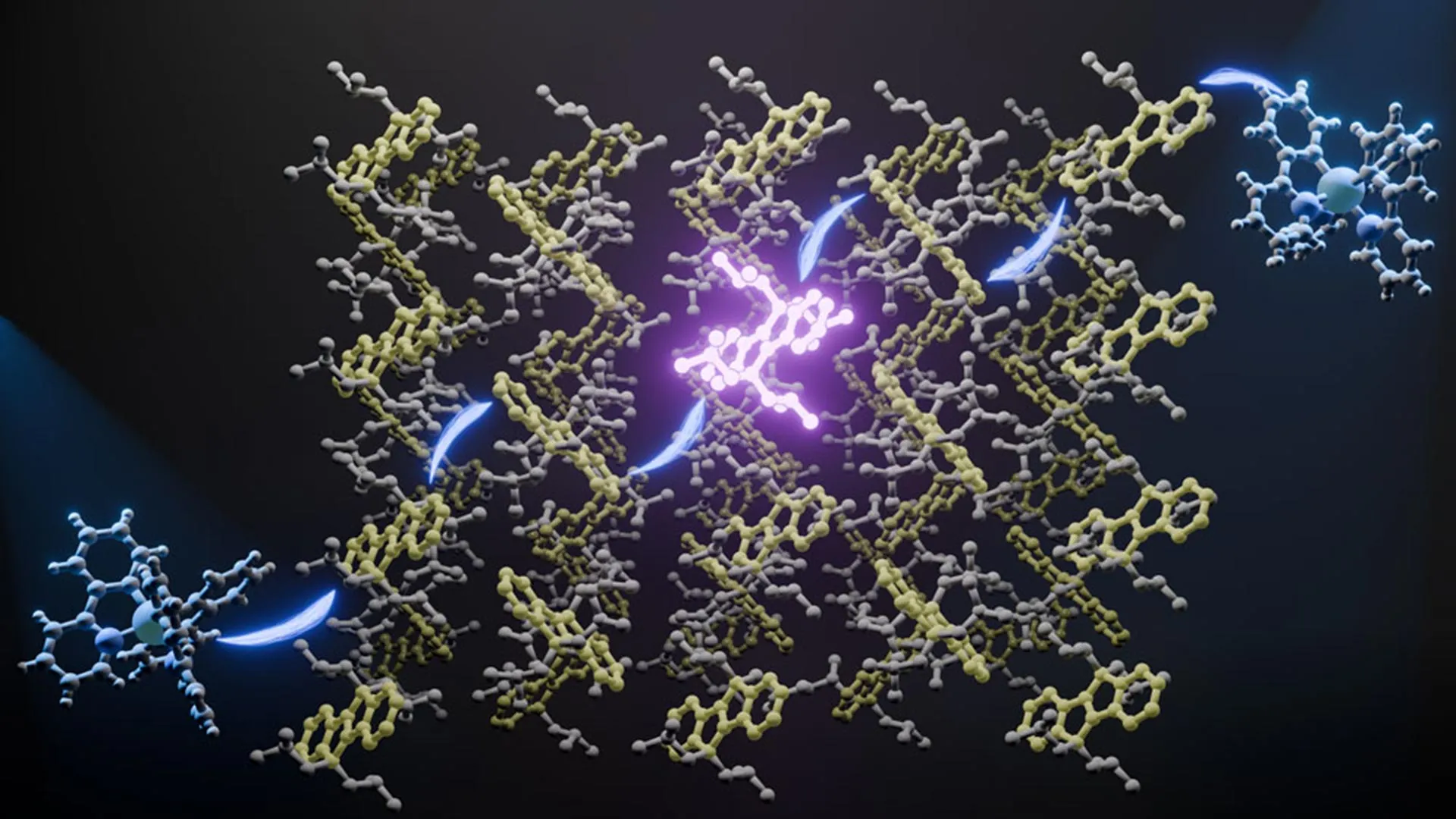
Both are limited by a basic problem: spin currents weaken as they travel through materials. Both also depend on spin mixing conductance, a measure of how efficiently spin passes across the boundary between a magnetic and a nonmagnetic material. Earlier studies showed that inserting an ultrathin layer at that boundary can raise the signals, but the mechanism was unclear.
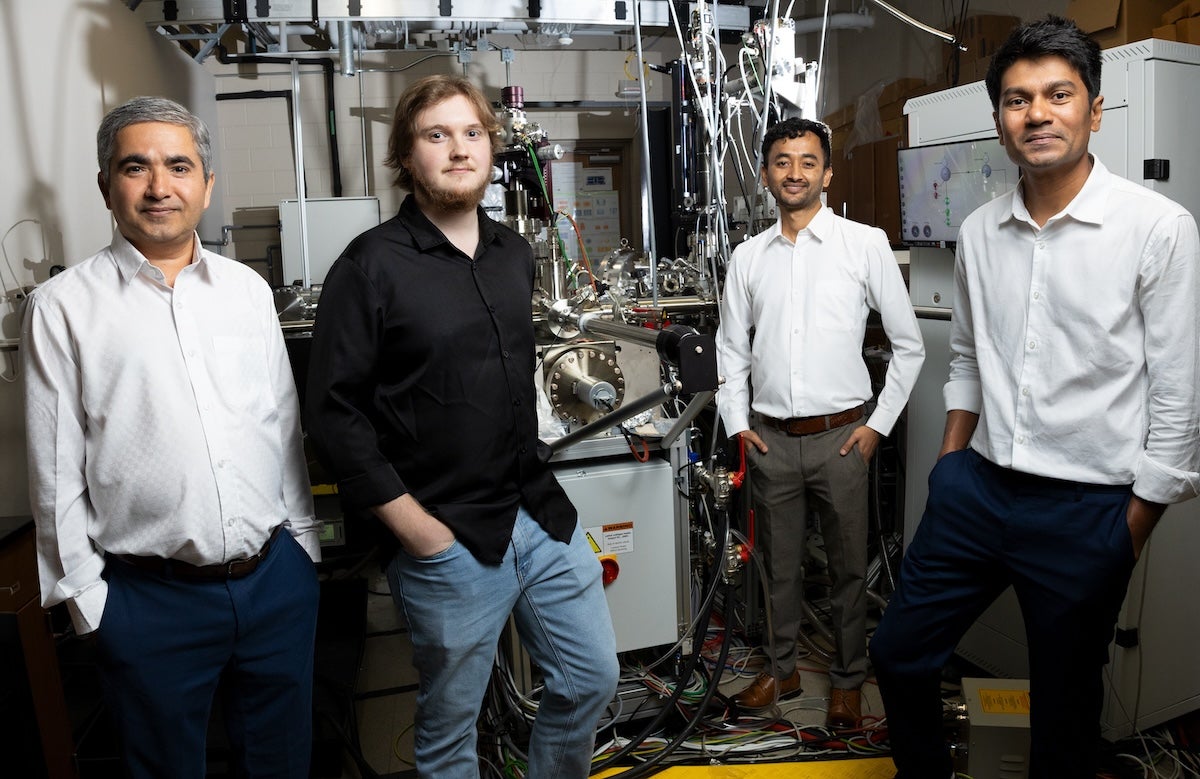
A team led by Professor Hiromi Yuasa of Kyushu University's Faculty of Information Science and Electrical Engineering built structures from yttrium iron garnet, or YIG, which served as the magnetic insulator, then IrMn, then platinum, which converted spin currents into electrical signals. They varied the IrMn thickness between 0 and 1 nanometer. Measuring both effects let them compare spin pumping, where spin angular momentum leaves the YIG layer, with spin absorption at an interface.
The strongest response in both the spin Seebeck voltage and the magnetoresistance came at 0.3 nanometers. The spin mixing conductance calculated from the two effects agreed well, which supports the conclusion that IrMn improves spin pumping and absorption through related interface mechanisms. At 0.3 nanometers the IrMn is expected to form islands rather than a continuous film. That structure may influence how spin transfers across the interfaces, though the team said more research is needed to sort out what each interface contributes.
The practical takeaway is that thickness and structure of an intermediate layer can be tuned to improve spin transfer. Yuasa pointed to battery-free information devices as one possible use. "By harnessing spin Seebeck power generation, these ultralow-power devices could operate without an external power supply or energy storage," he said, noting such devices would pose no risk of battery explosions.
"Our research could contribute to sustainable computing technologies based on novel principles, supporting the development of an unprecedentedly advanced information society," Yuasa said. The work is a laboratory measurement of material layers, not a finished device, and the gap between the two remains substantial.