Nanometer Changes in Metal Films Unlock Dramatic Electronic Control
University of Minnesota discovery shows how tiny thickness adjustments can alter metal properties by more than one electron volt.

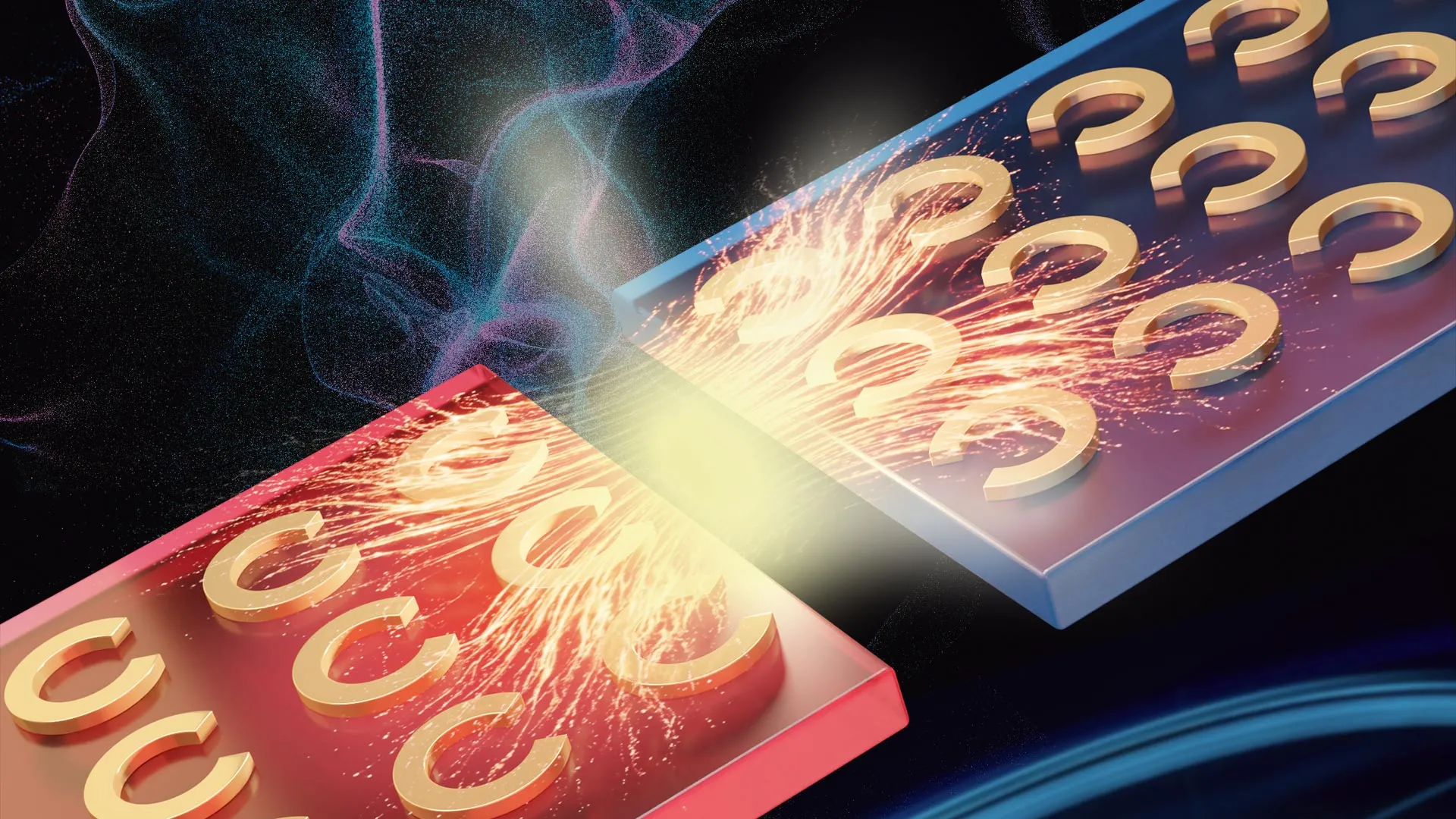
Scientists at the University of Minnesota Twin Cities have demonstrated an unexpected new approach to controlling the electronic properties of metals by engineering atomic-scale interactions at material interfaces. The research, published in Nature Communications, shows that interfacial polarization can dramatically alter the behavior of metallic ruthenium dioxide, achieving changes of more than one electron volt simply by adjusting film thickness by a few nanometers.
The breakthrough challenges conventional understanding of how metals behave and opens new possibilities for electronic device design. Professor Bharat Jalan, who holds the Shell Chair in the Department of Chemical Engineering and Materials Science, explained that polarization effects are typically associated with insulating materials rather than metals. However, the team discovered a method to stabilize polarization within a metallic system and use it as a control mechanism for electronic properties.
The most dramatic changes occurred when the ruthenium dioxide film reached approximately 4 nanometers thick, roughly the width of a single DNA strand. At this critical thickness, the metal undergoes a transition from a strained state caused by the underlying substrate material to a more relaxed atomic arrangement. This transition directly correlates with measurable changes in the material's electronic characteristics, providing clear evidence that atomic organization within materials can have significant practical implications.
First author Seung Gyo Jeong noted the surprising nature of the results, explaining that while subtle interface effects were expected, the magnitude and controllability of the work function changes exceeded predictions. The ability to visualize polar atomic displacements at the atomic scale and connect them directly to electronic measurements represents a significant advance in understanding how interface engineering can be used to manipulate material properties.
The discovery has potential applications extending beyond fundamental physics research into practical technologies including electronics, catalysis, and quantum systems. By demonstrating that nanometer-scale thickness control can produce substantial changes in electronic behavior, the research provides a new tool for materials engineers seeking to design devices with specific properties. The work involved collaborations across multiple institutions including MIT, Texas A&M University, and international partners in South Korea.