Swedish Physicists Boost Superconductors by Sculpting the Surface Beneath Them
By etching nanoscale ridges into a substrate, a Chalmers University team kept an ultrathin film superconducting at higher temperatures and stronger magnetic fields — a step toward energy-efficient electronics.
Researchers in Sweden have found a surprisingly simple way to make a superconductor more robust: reshape the surface it sits on. By subtly sculpting the base beneath an ultrathin superconducting film, the team kept the material superconducting at higher temperatures and under far stronger magnetic fields than before.
The work, led by Floriana Lombardi at Chalmers University of Technology in collaboration with RISE Research Institutes of Sweden and other international partners, was published in the journal Nature Communications. The researchers worked with ultrathin films of a copper-oxide compound, YBa₂Cu₃O₇₋δ, a so-called high-temperature superconductor prized because it carries electricity without resistance at temperatures far above those required by conventional superconductors.
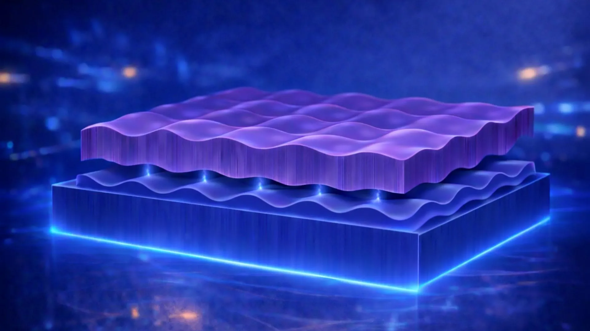
The trick lies in the substrate. The team pre-treated a supporting base of magnesium oxide in a vacuum at high temperature, coaxing it to form a regular pattern of tiny ridges and valleys — features smaller than one-millionth the thickness of a human hair. When the superconducting film was grown on top of this engineered landscape, the sculpted pattern guided the atomic arrangement and electron behavior within the film, stabilizing the fragile superconducting state.
That stability matters enormously for real-world use. Superconductors normally lose their special properties when warmed even slightly or exposed to strong magnetic fields, which has long limited where and how they can be deployed. By extending the range of temperatures and fields over which the thin film keeps working, the Chalmers approach edges these exotic materials closer to practical, everyday technology.
The implications reach across several fields. The researchers say the technique could help unlock ultra-energy-efficient electronics that waste little power as heat, next-generation quantum components for computing and sensing, and devices that depend on intense magnetic fields, such as advanced medical scanners and fusion reactors. Crucially, the method relies on shaping a common substrate rather than inventing an entirely new material — a practical advantage that could speed its adoption in laboratories and, eventually, industry.
Originally reported by ScienceDaily.