One Crystal, Three Jobs: Korean Team Chemically Turns a Single 2D Layer Into a Working Transistor
Published in Science, the method converts selected layers of tungsten diselenide into the semiconductor, insulator and metal-like contacts a transistor needs, with control near 0.7 nanometers.

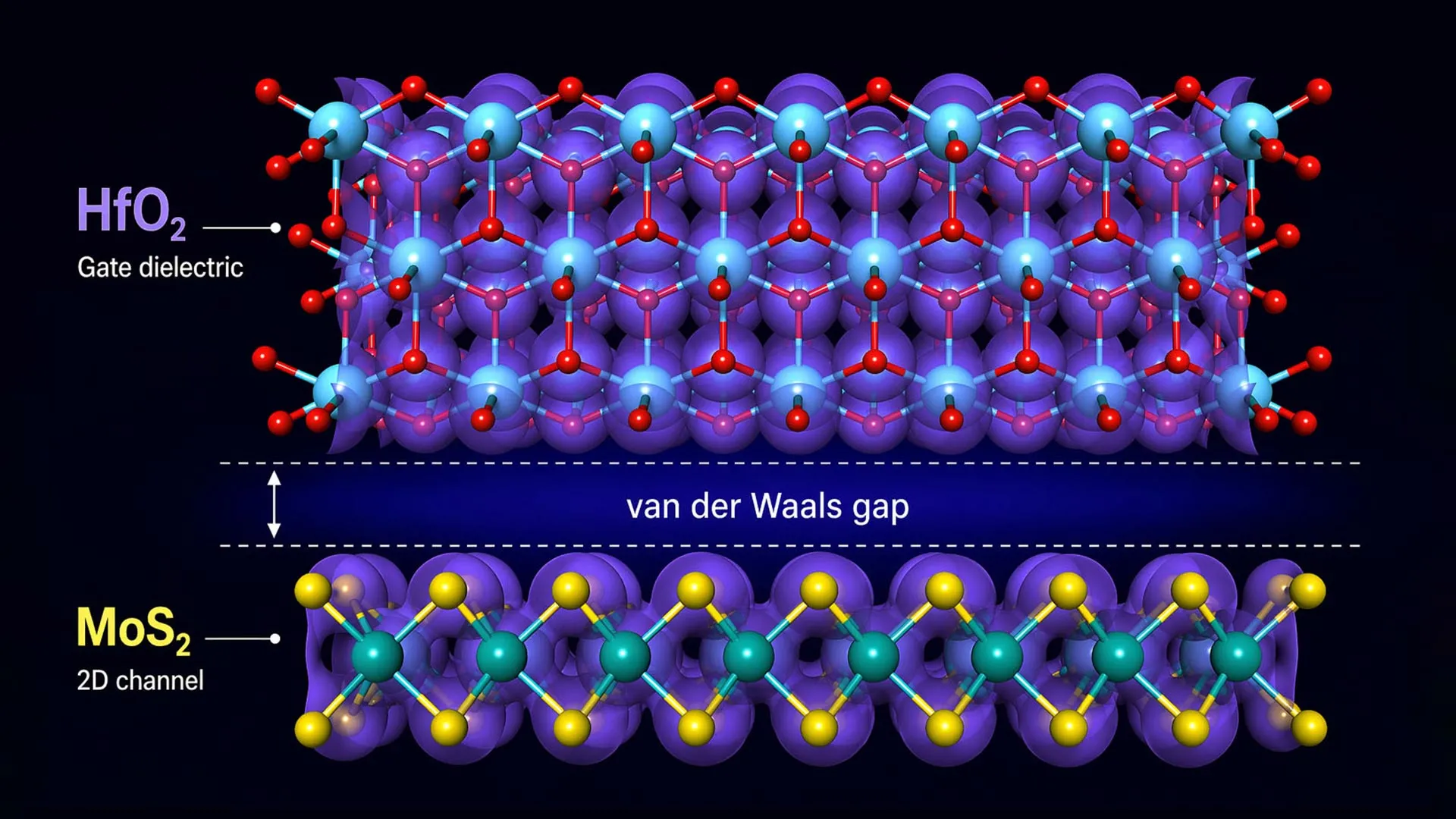
A transistor normally needs several fundamentally different materials: a semiconductor to carry current, an insulating dielectric to control it, and metallic contacts through which current enters and leaves. Fitting all of these together gets harder as devices shrink toward the atomic scale. A team in South Korea reports a different route: start with one layered crystal and chemically convert chosen layers and regions into each of the parts.
The work, led by Director Jo Moon-Ho of the Center for Van der Waals Quantum Solids at the Institute for Basic Science, is published in the journal Science. Instead of making the semiconductor, dielectric and contacts separately and then assembling them, the researchers used the crystal itself as the starting material for every electronic function.
Atomically thin two-dimensional semiconductors have long been seen as candidates to carry electronics past the scaling limits of silicon. According to the release, one of the biggest obstacles over more than two decades has not been the semiconductor itself but integrating it with other components. A transistor needs a highly uniform gate dielectric and low-resistance electrical contacts, yet the surfaces of 2D semiconductors have few sites where other materials can attach. That makes it hard to deposit conventional dielectrics evenly. Depositing metals directly can damage the atomically thin semiconductor or create large contact barriers that degrade performance. Peeling, positioning and stacking separate 2D materials by hand works in the lab but is difficult to scale across large areas and poorly suited to mass production.
The team began with multilayer tungsten diselenide, or WSe2, a 2D semiconductor. Its electrical properties can be changed by replacing some of the atoms surrounding the tungsten layer. By keeping the tungsten framework intact while selectively swapping those surrounding atoms, the researchers altered the electronic character of individual regions without rebuilding the crystal.
First, the upper layers of WSe2 were oxidized into insulating tungsten oxide. That oxide could then be converted through vapor-phase reactions into tungsten disulfide, an n-type semiconductor, or tungsten ditelluride, a semimetal. Regions left untouched kept the original WSe2 semiconductor behavior. In this way semiconducting, insulating and semimetallic functions were created inside different layers and locations of the same parent crystal.
The tiny gaps between neighboring atomic layers helped the researchers limit how far each reaction spread. By adjusting reaction temperature and gas pressure, they could stop the conversion after a chosen number of layers, giving control at roughly 0.7 nanometers per WSe2 monolayer. The team used the approach to fabricate high-performance modular integrated devices, as the release describes.
The announcement does not claim a commercial process. It is a materials-level demonstration published in a peer-reviewed journal, and questions about large-scale uniformity and manufacturing remain open. But if the conversion can be repeated reliably, building the whole device out of one crystal would sidestep the interface problems that have dogged 2D electronics.